NVIDIA introduced a pivotal breakthrough in AI technology by unveiling its next-gen Blackwell-based GPUs at the NVIDIA GTC 2024.
As the AI and machine learning sectors continue to evolve at a breakneck pace, NVIDIA’s latest innovation, the Blackwell architecture, is set to redefine AI and HPC with unmatched parallel computing capabilities.
NVIDIA showcased a new set of technologies that promise to accelerate AI training and inference like never before. They unveiled the Blackwell GPUs, the GB200 Super Chip, and the GB200 NVL72. Each represents groundbreaking innovation.
In this article, we’ll break down NVIDIA’s Blackwell architecture. What does it represent for high-performance computing, and how does it improve the Hopper architecture? Then, we will unpack each of the new products.
While NVIDIA’s Hopper architecture set a new standard for AI and accelerated computing in 2022, Blackwell takes things to another level. But what makes each of these architectures unique and how do they stack up against each other? In this blog, we’ll explore the key differences between NVIDIA Hopper and Blackwell, and which is best suited for your AI and HPC projects.
As AI advances, we’ll need more highly dense, incredibly powerful AI processors, which suggests that air cooling in server rooms may become obsolete.
Let’s talk about Blackwell, water cooling, and why Lenovo’s Neptune solution stands out at the moment. We’ll close with my Product of the Week: Microsoft’s Windows 365 Link, which could be the missing link between PCs and terminals that could forever change desktop computing.
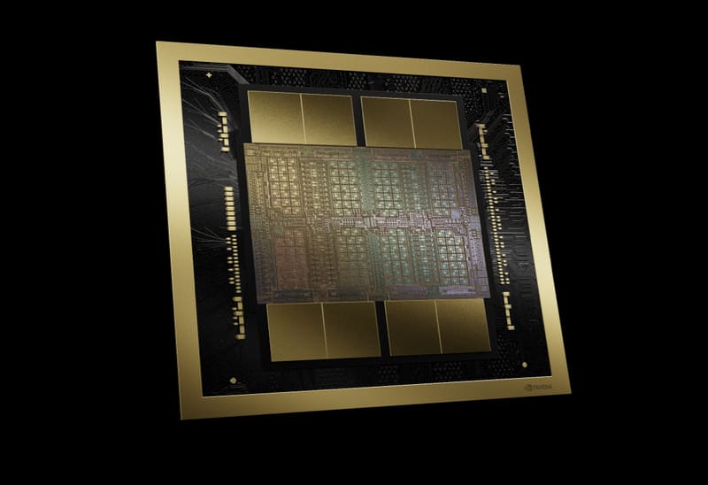
Blackwell
Blackwell is Nvidia’s premier, AI-focused GPU. When it was announced, it was so far over what most would have thought practical that it almost seemed more like a pipe dream than a solution. But it works, and there is nothing close to its class right now. However, it is massively dense in terms of technology and generates a lot of heat.
Some argue it is a potential ecological disaster. Don’t get me wrong, it does pull a lot of power and generate a tremendous amount of heat. But its performance is so high compared to the kind of load that you’d typically get with more conventional parts that it is relatively economical to run.
It’s like comparing a semi-truck with three trailers to a U-Haul van. Yes, the semi will get comparatively crappy gas mileage, but it will also hold more cargo than 10 U-Haul vans and use a lot less gas than those 10 vans, making it more ecologically friendly. The same is true of Blackwell. It is so far beyond its competition in terms of performance that its relatively high energy use is below what otherwise would be required for a competitive AI server.
But Blackwell chips do run hot, and most servers today are air-cooled. So, it shouldn’t be surprising that some Blackwell servers were configured with air cooling and those with 72 or more Blackwell processors on a rack overheated. While 72 Blackwells in a rack is unusual today, as AI advances, it will become more common, given Nvidia is currently the king of AI.
You can only go so far with air-cooled technology in terms of performance before you have to move to liquid cooling. While Nvidia did respond to this issue with a water-cooled rack specification that Dell is now using, Lenovo was way ahead of the curve with its Neptune water-cooling solution.
NVIDIA Blackwell GPU is capable of 20 petaFLOPS for accelerating HPC workloads and powering an innumerable number of operations per second. But the NVIDIA Blackwell GPU is quite not a one GPU… Instead, NVIDIA’s innovation in chip-to-chip interconnect has NVIDIA butting two GPU dies together to form a coherent bond merging two dies into a single unified GPU.
The entire Blackwell GPU consists of 208 billion transistors built on TSMC 4NP process (proprietary for NVIDIA) and is the Blackwell is a largest GPU ever. Each single GPU die is the largest die possible at TSMC’s within the limits of reticle size, and merging the two together only doubles what is capable. The NVIDIA High-Bandwidth Interface (NV-HBI) delivers 10TB/s of bidirectional bandwidth, effectively creating one single GPU out of two.
At a glance NVIDIA Blackwell features several new innovations
- Second Generation Transformer Engine – dynamic range management algorithms and fine-grain scaling techniques, called micro-tensor scaling, to optimize performance and accuracy
- Fifth Generation NVLink – 1.8TB/s bidirectional bandwidth per GPU with options for scalability of up to 576 GPUs. Additional GPUs interconnected via InfiniBand
- Decompression Engine – Accelerate database workloads and queries, paramount of enabling GPU accelerated data processing/analytics
- RAS Engine – Dedicated reliability, availability, and serviceability engine which employs AI for notifyin maintenance, enhancing system uptime, and reducing operating costs
The table below shows the NVIDIA Hopper vs NVIDIA Blackwell specs:
| Feature | NVIDIA Hopper Architecture | NVIDIA Blackwell Architecture |
| Transistor Count | 80 billion transistors | 208 billion transistors |
| Manufacturing Process | TSMC 4N process | Custom-built TSMC 4NP process |
| Transformer Engine | First-generation | Second-generation |
| Decompression Engine | No | Yes
|
| Energy Efficiency | Improved over the previous generation | 25x more energy-efficient than Hopper |
| Interconnect Technology | Fourth-generation NVLink | Fifth-generation NVLink |
| Chip-to-Chip Interconnect | 900 GB/s | 10 TB/s |
| Applications | Generative AI, LLMs, Data processing, Quantum computing | Accelerated Computing, AI, LLM |
2nd Gen Transformer Engine
Blackwell introduces the new second-generation Transformer Engine. The second-generation Transformer Engine uses custom Blackwell Tensor Core technology combined with TensorRT-LLM and Nemo Framework innovations to accelerate inference and training for LLMs and Mixture-of-Experts (MoE) models.
The Blackwell Transformer Engine utilizes advanced dynamic range management algorithms and fine-grain scaling techniques, called micro-tensor scaling, to optimize performance and accuracy and enable FP4 AI. This doubles the performance with Blackwell’s FP4 Tensor Core, doubles the parameter bandwidth to the HBM memory, and doubles the size of next-generation models per GPU.
With the Blackwell second-generation Transformer Engine, enterprises can use and deploy state-of-the-art MoE models with affordable economics, optimizing their business with the benefits of generative AI. NVIDIA Blackwell makes the next era of MoE models possible— supporting training and real-time inference on models over 10-trillion-parameters in size.
NVIDIA Blackwell Features to Power Generative AI
NVIDIA Blackwell GPUs are powered by six revolutionary technologies that will enable AI training and real-time LLM inference for models scaling up to 10 trillion parametres. The ground-breaking GPU will include the following features:
- Blackwell chip: The Blackwell processor packs 208 billion transistors and is manufactured using a custom-built 4NP TSMC process. All NVIDIA Blackwell products feature two dies that are linked via a 900GB/s chip-to-chip interconnect, providing the power of two GPUs in one fully cache-coherent, full-stack-ready blackwell chip.
- Generative AI Engine: Custom Tensor Core technology, combined with NVIDIA TensorRT-LLM and NeMo framework innovations, accelerates inference and training for LLMs, including a mixture-of-experts models. Enterprises can optimise their business with the latest expert parallelism and quantisation techniques and deploy these models by using new precision formats.
- Secure AI: Advanced confidential computing capabilities protect AI models and customer data with uncompromised performance, with support for new native interface encryption protocols, which are critical for data-sensitive industries like healthcare and financial services.
- Fifth-Generation NVLink: To accelerate performance for multitrillion-parameter AI models, NVLink’s latest iteration delivers ground-breaking 1.8 Tb/s throughput per GPU, ensuring seamless high-speed communication among up to 576 GPUs for today’s most complex large language models.
- Decompression Engines: Dedicated decompression engines support the latest formats, accelerating database queries to deliver the highest performance in data analytics and data science.
- RAS Engine: Only Blackwell-powered GPUs include a dedicated engine for reliability, availability and serviceability.
The Blackwell architecture offers improved performance with:
FP8 Performance: The Blackwell architecture offers 20 PetaFLOPS (PFLOPS) of performance at FP8 precision, which is 2.5 times the performance of the Hopper architecture.
- FP6 Performance: Like FP8, FP6 performance on the Blackwell architecture is also 20 PFLOPS, a 2.5-time improvement over the Hopper architecture.
- FP4 Performance: This is a significant leap, with Blackwell offering 40 PFLOPS in the new FP4 metric, five times the performance of Hopper. This indicates a strong emphasis on improving performance for lower-precision computations, which are crucial for AI inference.
- HBM Model Size: NVIDIA’s Blackwell architecture supports models up to 740 billion parameters in size, which is six times larger than what Hopper architecture could manage. This massive increase supports the development and operation of larger and more complex AI models.
- HBM Bandwidth: The High-Bandwidth Memory (HBM) bandwidth on Blackwell is 34 Terabytes per parameter second (TB/s), which is five times the bandwidth available on Hopper. This allows for faster data transfer rates, which significantly improves computing performance.
- NVLink All-Reduce with SHARP: The Blackwell architecture offers 7.2 TB/s NVLink all-reduce capabilities with SHARP technology, four times the capability of Hopper architecture. SHARP (Scalable Hierarchical Aggregation and Reduction Protocol) enhances collective communication operations, which is crucial for distributed AI and machine learning tasks.
NVIDIA Blackwell was released in 2024 and named after David Harold Blackwell, a renowned statistician and mathematician whose work in probability theory and dynamic programming has had a lasting impact on computational sciences. Blackwell’s contributions to the field of mathematical statistics align with the architecture’s focus on generative AI, LLMs, and data-centric workloads.
The NVIDIA GB200 GPU from the Blackwell series boasts 208 billion transistors and HBM3e memory, offering a massive leap in performance compared to the Hopper series. With up to 20 petaflops of AI performance, Blackwell is designed to handle the most demanding computational tasks, such as training large AI models, running complex simulations, and accelerating generative AI applications.
One of Blackwell’s standout features is its dedicated decompression engine, which speeds up data processing by up to 800 GB/s—making it 6x faster than Hopper when dealing with large datasets. Blackwell also enhances Confidential Computing, ensuring a secure and efficient environment for sensitive AI workloads, while introducing breakthroughs in quantum simulations and scientific research, making it the next frontier in AI and HPC computing.
About NVIDIA Blackwell GPUs: B100 and B200
Based on the Blackwell architecture NVIDIA, the NVIDIA B200 Tensor Core GPU delivers a massive leap forward in speeding up inference workloads, making real-time performance a possibility for resource-intensive and multitrillion-parameter language models.
Two B200 GPUs are combined in Blackwell’s flagship accelerator, the NVIDIA GB200 Grace Blackwell chip, which also utilises an NVIDIA Grace CPU. The GB200 provides a 30x performance increase compared to the NVIDIA H100 Tensor Core GPU for LLM inference workloads and reduces cost and energy consumption by 25x.
For the highest AI performance, GB200 supports the NVIDIA Quantum-X800 InfiniBand and Spectrum™-X800 Ethernet platforms which deliver advanced networking options at speeds up to 800 Gb/s. The GB200 NVL72 also includes NVIDIA BlueField®-3 data processing units to enable cloud network acceleration, composable storage, zero-trust security and GPU compute elasticity in hyperscale AI clouds.
The GB200 is a key component of the NVIDIA GB200 NVL72, a multi-node, liquid-cooled, rack-scale platform for the most compute-intensive workloads. It combines 36 Grace Blackwell chip, which include 72 B200 GPUs and 36 Grace CPUs interconnected by fifth-generation NVLink.
To help accelerate the development of Blackwell-based servers from its partner network, NVIDIA announced NVIDIA HGX B200, a server board that links eight B200 GPUs through high-speed interconnects to develop the world’s most powerful x86 generative AI platforms. HGX B200 supports networking speeds up to 400 Gb/s through the Quantum-2 InfiniBand and Spectrum-X Ethernet platforms, along with support for BlueField-3 DPUs.
NVIDIA B100 and B200
NVIDIA is building on the Blackwell architecture by introducing two new GPUs, the B100 and B200. These GPUs feature a dual-die design, with each die containing four HBM3e memory stacks offering 24GB per stack and a bandwidth of 1 TB/s on a 1024-bit interface.
The B100 and B200 GPUs also improve the precision of floating-point operations. They come with a transformer engine that dynamically and automatically rescales and recasts numerical precision to a lower format whenever possible. This improves machine learning computations because when dealing with small floating-point numbers, the accuracy of the calculations affects the ability and accuracy of machine learning models.
| SPECIFICATION | HGX B200 | HGX B100 |
|---|---|---|
| GPUs | HGX B200 8-GPU | HGX B100 8-GPU |
| Form factor | 8x NVIDIA B200 SXM | 8x NVIDIA B100 SXM |
| HPC and AI compute (FP64/TF32/FP16/FP8/FP4)* | 320TF/18PF/36PF/72PF/144PF | 240TF/14PF/28PF/56PF/112PF |
| Memory | Up to 1.5TB | Up to 1.5TB |
| NVIDIA NVLink | Fifth generation | Fifth generation |
| NVIDIA NVSwitch™ | Fourth generation | Fourth generation |
| NVSwitch GPU-to-GPU bandwidth | 1.8TB/s | 1.8TB/s |
| Total aggregate bandwidth | 14.4TB/s | 14.4TB/s |
NVIDIA B100
The B100 Blackwell GPU provides balanced computational efficiency. It delivers up to 7 PFLOPS for dense FP4 tensor operations, where ‘dense’ implies that most of the tensor’s elements are non-zero, necessitating comprehensive computation. In contrast, it achieves up to 14 PFLOPS for sparse FP4 operations, where ‘sparse’ indicates that most elements are zero, allowing for optimized, faster processing due to fewer non-zero elements needing calculation.
For FP6/FP8 tensors, essential in balancing precision and computational speed, the B100 reaches 3.5/7 PFLOPS for dense/sparse tasks, respectively. Its INT8 tensor performance, critical for fast data inference, stands at 3.5/7 POPS for dense/sparse scenarios.
In higher accuracy requirements, the B100’s FP16/BF16 tensors operate at 1.8/3.5 PFLOPS for dense/sparse, and TF32 tensors at 0.9/1.8 PFLOPS, supporting a range of precise computing tasks. Furthermore, it offers 30 TFLOPS in FP64 dense computations for scientific applications requiring the utmost accuracy.
The GPU has 192GB of memory, facilitating substantial data handling. It supports an 8 TB/s memory bandwidth and an equivalent 1.8 TB/s NVLink bandwidth for swift data communication. With a 700W power specification, the B100 stands out as an energy-efficient option for complex computational setups requiring balanced power and performance.
NVIDIA B200
The B200 Blackwell GPU achieves up to 9 PFLOPS in dense and 18 PFLOPS in sparse FP4 tensor operations. For FP6/FP8 tensor operations, balancing precision and speed, the B200 records 4.5/9 PFLOPS for dense/sparse activities, respectively. Its INT8 tensor capability, important for quick data analysis and inference, reaches 4.5/9 POPS for dense/sparse computations, ensuring efficient real-time processing.
The B200 would shine in precision tasks with 2.25/4.5 PFLOPS for dense/sparse FP16/BF16 tensors and 1.2/2.25 PFLOPS for dense/sparse TF32 tensors, suitable for various scientific and machine learning applications. For ultimate precision, such as in detailed scientific calculations, it offers a solid 40 TFLOPS in FP64 dense computations.
| SPECIFICATION | B100 (Dense) | B100 (Sparse) | B200 (Dense) | B200 (Sparse) |
|---|---|---|---|---|
| Configuration | Blackwell GPU | Blackwell GPU | Blackwell GPU | Blackwell GPU |
| FP4 Tensor | 7 PFLOPS | 14 PFLOPS | 9 PFLOPS | 18 PFLOPS |
| FP6/FP8 Tensor | 3.5 PFLOPS | 7 PFLOPS | 4.5 PFLOPS | 9 PFLOPS |
| INT8 Tensor | 3.5 POPS | 7 POPS | 4.5 POPS | 9 POPS |
| FP16/BF16 Tensor | 1.8 PFLOPS | 3.5 PFLOPS | 2.25 PFLOPS | 4.5 PFLOPS |
| TF32 Tensor | 0.9 PFLOPS | 1.8 PFLOPS | 1.2 PFLOPS | 2.25 PFLOPS |
| FP64 Tensor | 30 TFLOPS | – | 40 TFLOPS | – |
| Memory | 192GB (8x24GB) | 192GB (8x24GB) | 192GB (8x24GB) | 192GB (8x24GB) |
| Bandwidth | 8 TB/s | 8 TB/s | 8 TB/s | 8 TB/s |
| NVLink Bandwidth | 1.8 TB/s | 1.8 TB/s | 1.8 TB/s | 1.8 TB/s |
| TDW | 700W | 700W | 1000W | 1000W |
Equipped with 192GB of memory, the B200 enhances large-scale data processing. It is supported by an 8 TB/s memory bandwidth and a corresponding 1.8 TB/s NVLink bandwidth, facilitating fast and efficient data transfer. With a power consumption rated at 1000W, the B200 is designed for energy efficiency in demanding computational environments, balancing high-end performance and power usage.
NVIDIA Blackwell Series GB200
The NVIDIA Blackwell GB200 NVL/72 36 GPU shows a major leap in generative AI and accelerated computing. Built using 208 billion transistors and featuring HBM3e memory, the NVIDIA GB200 NVL/72 36 provides massive computational power for AI training, inference, and large-scale simulations.
Key NVIDIA Blackwell features of NVIDIA GB200 NVL/72 36 include:
- Second-generation Transformer Engine with new micro-tensor scaling techniques for FP4 precision, doubling the performance of next-gen AI models while maintaining high accuracy.
- 10 TB/s chip-to-chip interconnect, enabling faster data communication within multi-die GPUs for enhanced generative AI processing.
- NVIDIA Decompression Engine, delivering up to 900 GB/s bandwidth, significantly accelerating data processing for large datasets and analytics workloads.
- Confidential Computing capabilities, protecting sensitive AI models with hardware-based security and TEE-I/O integration.
With up to 20 petaflops of AI performance, Blackwell is ideal for generative AI models, LLMs, and high-performance scientific computing.
When are NVIDIA Blackwell GPUs Coming Out?
The highly anticipated NVIDIA Blackwell chip GB200 NVL72/36 is expected to be available by the end of 2025. These cutting-edge GPUs are designed to deliver exceptional performance for AI and high-performance computing (HPC) workloads. We are one of the first Elite Cloud Partners in the NVIDIA Partner Network to offer NVIDIA Blackwell platform-powered compute services. You can reserve the NVIDIA GB200 NVL72/36 in advance on the AI Supercloud and secure early access to the fastest performance for your AI projects. By reserving now, you’ll be among the first to leverage Blackwell’s unmatched capabilities in generative AI and large-scale model training.